What is Shadow Masking?
In semiconductor fabrication, stencil metal plates or shadow masks can be used to designate where a metal is deposited upon a substrate. The stencil serves as a medium for achieving custom designs onto a substrate without the need for photolithography processes. This works by masking certain areas of a substrate while exposing others to be deposited with metal.
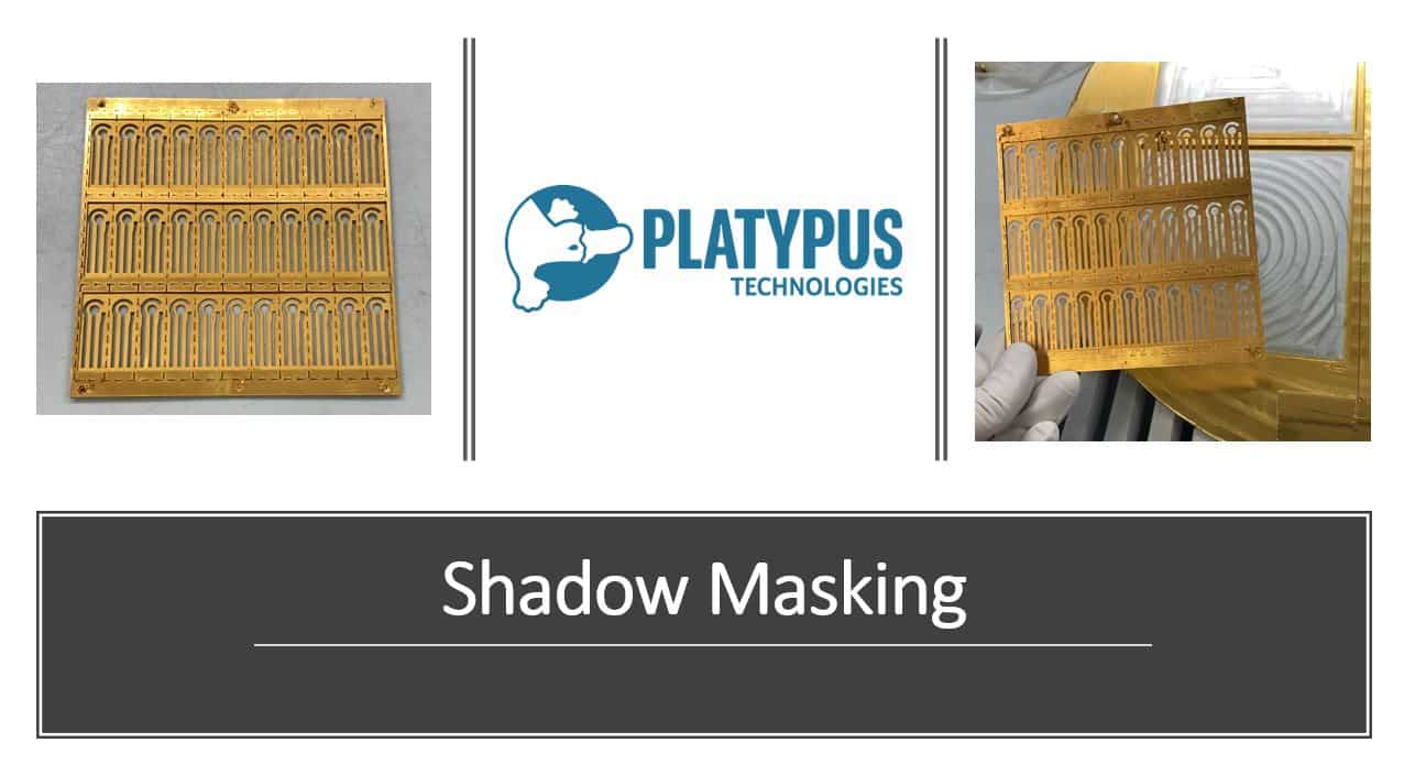
Shadow masks are typically made with thin stainless steel or nickel sheet metal. Creating shadow masks can be quite difficult, as the required machining can be difficult to obtain and result in jagged edges. For high precision designs, shadow masking may present some difficulties. Small feature sizes are often harder to obtain with shadow masking when compared to photolithography fabrication methods. Shadow masks are more well-suited for low resolution (>0.7 mm) applications. In photolithography, designs are transferred onto a substrate through a photomask and UV exposure. However, photolithography processes often result in higher manufacturing costs. Photolithography production relies on patterning via photoresist application and a form of removal of unwanted areas (metal lift-off or wet etching). These processes require expensive photoresists and solvents, where substrate materials can be subjected to increased amounts of errors due to a range of variable factors.
Shadow masking offers a more mechanical mechanism for transferring designs by using a metal stencil that can be directly used in vacuum chamber evaporation processes. Fixturing a substrate and shadow mask into a vacuum chamber also presents a challenge. As opposed to typical fixturing methods, magnets can be used to keep both the substrate and shadow mask in place. The strength of the magnet can determine the degree to surface contact between the mask and substrate. The stronger magnet will result in direct surface contact between materials. Following metal deposition, a mask is lifted off the substrate to reveal a pattern. Shadow masking can significantly reduce production costs by providing a more reproducible method for creating custom patterned surfaces. As opposed to photolithography, shadow masking does not require the need for pricey photoresists and solvents.
Fabricating microelectronic devices can be done via shadow masking. Shadow masking offers a highly reproducible method that creates a low surface roughness, high purity metal coated surface. Applications include creating custom patterned electrodes, sensors, bonding pads, MEMs devices, and more.
At Platypus Technologies, we have worked to optimize our shadow masking services to achieve better results. We offer customizable shadow masking services for metal coatings. Simply provide us with your design where we will replicate it onto a thin metal stencil. Customer specified substrate materials will then be coated through our custom metal deposition services through physical vapor deposition. Our capabilities comply with small batch projects like prototyping. Contact us today at