Gold Coated Silicon Wafers And Chips
Silicon wafers and chips coated with 99.999% pure gold are ideal substrates for characterization of materials via Spectroscopy, Microscopy and Electrochemistry. Our products are engineered for precision and consistency, offering researchers and scientists a reliable foundation for groundbreaking discoveries.
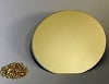 Gold Coated Silicon Wafers
Product Overview: Our Silicon Wafers, 100-mm prime-grade discs with a 525 µm thickness, feature gold thin films layered over a titanium adhesion layer. These wafers are designed for precision and reliability in various scientific research settings.
Available in different pack sizes for diverse analytical requirements. Ensures enhanced conductivity and durability for electrochemical experiments, as well as superior reflectivity, ideal for detailed spectroscopic analysis.
Available Variants: 50-nm Gold film OR 100-nm Gold film. Contact us for custom thickness of gold film.
| Description | |
|---|---|
| Silicon Wafer coated with 50-nm gold – 1 wafer | BUY NOW |
| Silicon Wafer coated with 50-nm gold – 3 wafers | BUY NOW |
| Silicon Wafer coated with 100-nm gold – 1 wafer | BUY NOW |
| Silicon Wafer coated with 100-nm gold – 3 wafers | BUY NOW |
| Silicon Wafer coated with 100-nm gold – 12 wafers | BUY NOW |
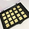 Gold Coated Silicon Chips
Square chips of silicon with dimensions with 10-mm x 10-mm x 0.525-mm are coated with a 100-nm gold film over a titanium adhesion layer. Gold coated chips are easy to handle and aid in waster reduction, especially in especially in experiments or processes where the entire surface area of a larger wafer would not be utilized.
If you need gold-coated silicon chips with alternative dimensions, please contact us.
Ordering in Bulk? Contact us for Special Pricing
| Description | |
|---|---|
| Silicon chips (10 mm x 10 mm) coated with 100-nm of gold – 20 chips | BUY NOW |
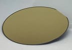 Gold Coated Thermal Oxide Silicon Wafers
Our silicon wafers are 100 mm discs with thickness of 525 µm, and thermal oxide layer thickness of 285-nm +/- 5%. Gold film coated over titanium adhesion layer (to promote mechanical stability of thin film). Ideal for fabrication for sensors, biosensors and electrodes via photolithography and wet etching techniques.
| Description | |
|---|---|
| Silicon wafer with thermal oxide layer, coated with 50-nm of gold – 1 wafer. | BUY NOW |
Customized Solutions
Looking for bulk orders or specific requirements? Contact us for special pricing and bespoke solutions tailored to your research needs.
Applications
Our premium gold-coated silicon wafers feature a thin titanium adhesion layer that enhances the gold layer’s adherence to the silicon base, ensuring durability and reliability. Platypus Technologies gold coatings feature 99.999% pure gold for superior electrical conductivity and optical reflectivity.
Ideal for a range of scientific applications, these gold-coated wafers serve as perfect substrates for analytical characterization of materials in chemistry, biochemistry and nanotechnology. They are extensively used in thin film analysis, nanoparticle research, protein studies, and self-assembled monolayers. Their compatibility with diverse spectroscopic techniques, including electrochemistry, IR spectroscopy, Raman spectroscopy, X-ray spectroscopy, and ellipsometry, makes them a versatile choice for researchers and scientists.
For example, materials deposited onto gold-coated wafers can be analyzed via ellipsometry, Raman spectroscopy or infrared (IR) spectroscopy due to the high-reflectivity and favorable optical properties of gold.
Moreover, our gold-coated silicon wafers are indispensable in the fabrication of complex electrochemical devices. They are a preferred choice for creating advanced electrodes, electrochemical sensors, and photonic devices, thanks to their high reflectivity and favorable optical properties. These wafers are also ideal for developing self-assembled monolayers and other cutting-edge technologies.
Discover the potential of gold-coated silicon chips and wafers in your research and development projects. Their extensive application in material characterization, especially through ellipsometry, Raman spectroscopy, and IR spectroscopy, highlights their adaptability and efficiency in scientific exploration and technological innovation. Choose our gold-coated silicon wafers for unparalleled performance in your advanced research and manufacturing needs.
Studies that utilized gold coated wafers:
- Electrochemical Impedance of polyamide thin films
- Nanomaterials formed by cyclic β-peptide polymers
- Two-Photon Photochroism in Metasurface Absorbers
- Bacteriophage-based photonic nose for cell recognition
- Patterning monolayers via lift-off lithography
- Nanoparticles for enhanced Raman spectroscopy
Related: Additional published studies utilizing gold-coated silicon wafers
Blogs on gold coated wafers
- Gold-Coated Silicon Wafers: Properties & Applications
- Gold-Coated Silicon Wafers in Electrochemistry
- Electrochemical Analysis of Dyes with Gold Electrodes
Don’t see what you need? Contact us for custom gold coating projects on 608-237-1270 or email us.
Frequently Asked Questions
Orientation: <100>
Grade: Prime
Polishing: Single-side
Roughness: 2-3 angstrom
Dimensions: 100-mm diameter
Thickness: 525 +/- 25 μm
Dopant Type: P (Boron)
Resistivity: 1-20 ohm-cm
Gold-coated wafers exhibit optical reflection >90% for wavelengths of light greater than 580-nm. At 800-nm, for example, the reflectivity is well above 99%. To learn more about the reflectivity of gold films, please review our blog on optical reflection of gold thin films.
Gold thin films with thickness of 100-nm have a sheet resistance of 240 milliohm/sq. The bulk resistivity of the silicon wafer is approximately 1-20 ohm-cm.
Yes. We can provide gold-coated chips with dimensions as small as 7-mm x 7-mm, and gold-coated wafers as large as 200-mm diameter. For gold deposition, we can coat films as thin as 5-nm and as thick as several micrometers. Please contact us for your custom request
1 – 2 weeks, depending on the complexity of the project.
To ensure the quality and consistency of our gold coated silicon products at Platypus Technologies, we implement a rigorous quality control process that includes:
1. Optical Characterization: We perform comprehensive optical tests to assess the uniformity and thickness of the gold coatings. This ensures that each product meets our high standards for optical properties, which are crucial for their intended applications in spectroscopy and microscopy.
2. Electrical Characterization: Our gold thin films undergo detailed electrical testing. This step is essential to guarantee that the electrical properties of the films meet the precise requirements for electrochemistry applications.
3. Regular Equipment Maintenance: The deposition equipment used for applying the gold layers is maintained regularly. This maintenance includes calibration and routine checks to ensure consistent film quality. Regular upkeep of our equipment is key to preventing any variability in the coating process.
By adhering to these stringent quality control measures, we at Platypus Technologies are committed to providing our customers with gold coated silicon products that consistently meet the highest standards of quality and reliability.