Gold-Coated Silicon Wafers: Properties & Applications
Since the 1960s, silicon technology has been revolutionizing the way we think about electronic devices and digital communications. Gold-coated silicon wafers represent another step on that exponential trajectory of innovation in semiconductor technology, combining the inherent electrical properties of silicon with the unique optical and physicochemical characteristics of gold. Provided the composite is engineered with absolute precision, gold-coated silicon wafers can be used in critical nanophotonic applications.
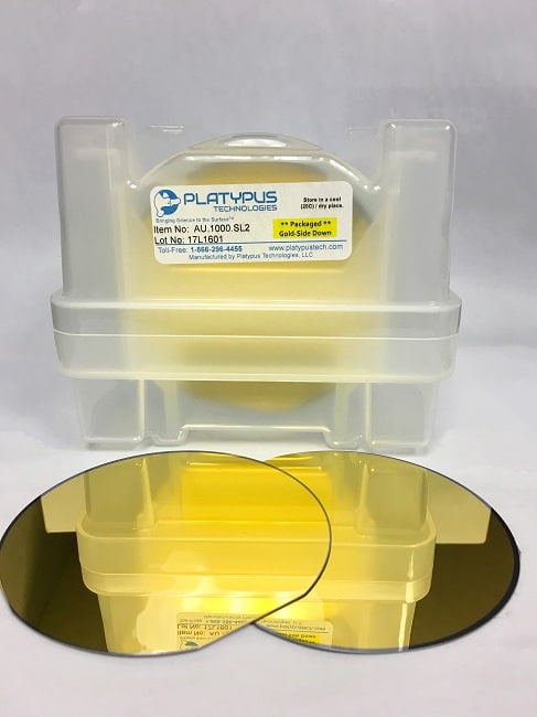
At Platypus Tech, we design and supply custom gold-coated silicon wafers based on years of surface science experience. We offer a core range of silicon chips and wafers coated with high-purity gold, which are routinely leveraged in electrochemistry, microscopy, and spectroscopy.
Gold-Coated Silicon Wafers: Properties & Characteristics
As mentioned, we primarily offer gold-coated silicon in two formats, but we will be focussing explicitly on our wafers throughout this article.
Our gold-coated silicon wafers are manufactured in a Class 10,000 cleanroom environment using intermediate products from quality-assured suppliers. We exclusively use 100 mm test-grade silicon discs as substrates with a thin titanium bonding layer on the surface. This adhesive is usually no thicker than 5 nanometres (nm) and is relative to the thickness of the gold thin film at an approximate ratio of 20:1.
Applications of Gold-coated Silicon Wafers
As with our gold-coated glass products, one of the main benefits of our silicon substrates is their planarity. We can engineer our gold-coated wafers with outstanding flatness, often approaching the angstrom range. This makes it the ideal substrate for increasing resolution and sensitivity in nanoscale imaging applications, such as in single-molecule infrared spectroscopy. The high reflectivity of gold to radiation on the infrared region of the electromagnetic spectrum makes it an extremely suitable material for resolving extremely small analytes under complex test parameters.
The functionalities of our gold-coated silicon wafers extend even further in studies of electrochemistry, as the coated substrate can serve as a high-performance electrode. Chemists can easily and reliably characterize reaction kinetics as a function of voltage; a technique with far-reaching analytical applicability.
Gold-Coated Silicon Wafers from Platypus Technologies
At Platypus Technologies, we operate on a customer-first design principle, which means all our gold-coated silicon wafers are manufactured on a custom made-to-order basis. If you are interested in using coated silicon wafers for your analytical procedures, why not contact a member of the team today to discuss partnership opportunities with us?