Patterning Metal Surfaces Using Shadow Masks
Surface patterning describes fabrication methods which modify substrates with extreme precision.
The need for detailed surface structures is becoming increasingly common for scientists across a range of disciplines and there are many means with which these surface patterns can be created.
In this blog, we discuss surface patterning with shadow masks, an important tool for fabricating thin film components for microelectronics in a rapid and repeatable manner.
What are Shadow Masks?
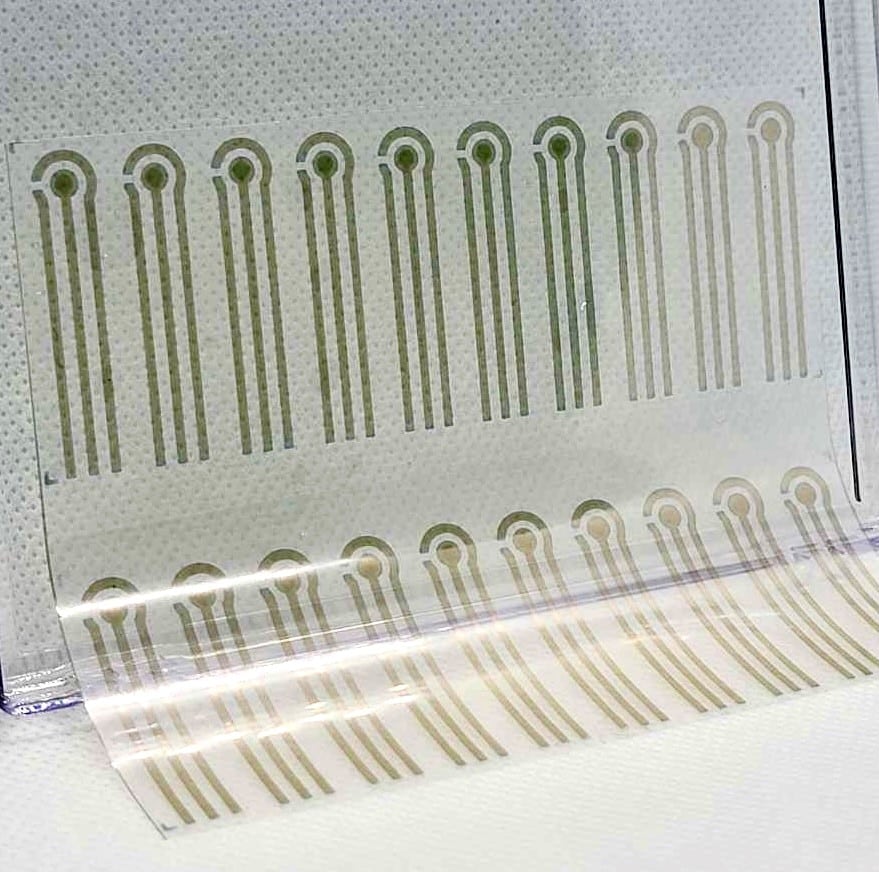
Shadow masks are metal sheets which have patterned holes cut into them. These sheets are then placed on top of a substrate such as glass, silicon or ceramics, or flexible films during metal deposition.
The pattern on the shadow mask determines the areas of the substrate that will be coated with metal, and the areas that will not be coated.
Shadow masking, coupled with e-beam metal deposition, is a one-step process for fabricating high-quality patterned electrodes, sensors, heating wires, bonding pads and other features commonly encountered in microelectronic devices.
Advantages of Shadow Masks
Unlike screen-printing methods which require organic inks, shadow masks used with e-beam metal deposition utilize metals with very high purity. Thus, the metal patterns produced with shadow masks have the following advantages:
- Very high reproducibility
- Low surface roughness (<5-nm)
- High purity metals (>99.999% for Au, Pt and other metals)
Screen printed features have residual organic materials from the inks often create unwelcome contamination. In addition, screen printing results in very rough edges and surface features, meaning that the results are far less repeatable and reproducible.
In comparison to photolithography-based methods for surface patterning, shadow masking does not require expensive photomasks, photoactivated materials, or expensive processing equipment such as hot plates, spin-coaters, and solvent benches. Shadow masking is easier to implement and results in lower cost compared to photolithography.
Shadow masks are well-suited for applications with relatively-low resolution (large features >250 µm). For fabricating fine features(1 to 250-µm) with tight tolerances, photolithography-based methods are recommended.
Surface Patterning with Shadow Masks at Platypus Technologies
At Platypus Technologies, we offer services in design, fabrication of shadow mask with custom patterns, metal deposition to create electrodes, sensors, heating lines and other circuit lines. We stock a range of metal surfaces (Au, Ag, Al, Pt, Ni, Ti, Cr) and substrates (glass, silicon, ceramic, flexible films) to produce custom coatings to suit your most complex project. Our dicing and cutting services singulate devices for plug-and-play applications. Contact us today to discuss your project!