Thin Film Interference Effects
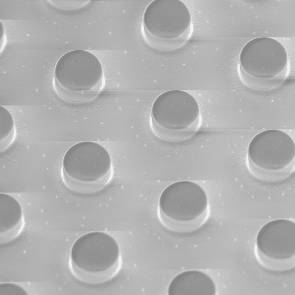
During the photolithography process, thin film interference effects can influence a substrates surface properties. Common interference effects include the standing wave effect, reflective notching, edge bead formation, and under/over baking. The Platypus Technologies engineers have enhanced our standard operating procedures to account for potential defects caused by thin film interference effects.
A phenomenon known as the standing wave effect occurs when reflected light from a substrate interferes with a light wave traveling downwards, causing a ripple like appearance to occur on a photoresist pattern. When a light wave strikes the surface of a photoresist, light is either transmitted or reflected. The amplitude of a standing wave depends on substrate reflectivity and resist absorption. Reducing the severity of standing waves can be done through anti-reflective coatings, and a post-exposure bake (PEB). Anti-reflective coatings have a high absorption of incident light which can help to reduce the reflectivity at the substrate and resist interface. The effectiveness of anti-reflective coatings depends on its thickness which can either be increased or decreased depending on the photoresist thickness. In addition, post-exposure baking can be used to reduce and eliminate standing wave formation. The high temperatures that are used during PEB initiate diffusion in both the exposed and unexposed photoproducts within a photoresist, creating a more uniform surface.
Reflective notching can also occur causing exposure in unwanted regions as well as irregular patterns. This is commonly encountered when working with Aluminum which has reflective surface properties that case interference effects. Adjusting photoresist composition can help to alleviate reflective notching through the addition of a dye. Anti-reflective coatings also contribute to reducing reflections.
Edge beads can accumulate on a substrate surface during spin coating due to surface tension. The presence of edge beads leads to contamination, wafer breakage, increased processing times, and inaccurate pattern transfer. Preventing edge beads is done through calculating appropriate spin speeds based on photoresist viscosity. Chemical edge bead remover (EBR) can be directly applied to the affected region of a substrate to effectively remove the impurity.
The soft and hard baking steps in the photolithography process may affect the adhesion between the photoresist and the substrate. Soft baking is performed directly following spin coating. Hard baking is commonly done after UV exposure. Under-baking causes inadequate resist to substrate adhesion where over baking can induce cracking and peeling. Depositing a metal adhesion layer can enhance substrate to metal adhesion. However, a more cost-effective solution is through UV ozone treatment. UV ozone has been shown to improve substrate adhesion by increasing metal to substrate bond strength by forming a monolayer on the metal surface [1]. Treating a substrate prior to metal deposition can increase surface wettability and surface roughness, contributing to improving metal to substrate adhesion [1].
The engineers at Platypus Technologies have conducted multiple QC experiments in order to optimize our photolithography processing and manufacturing. Contact us today to inquire about our photolithography services!
Resources:
[1] Hai Le-The, Roald M. Tiggelaar, Erwin Berenschot, Albert van den Berg, Niels Tas, and Jan C. T. Eijkel. ACS Nano 2019 13 (6), 6782-6789. DOI: 10.1021/acsnano.9b01403