Using Photolithography to Pattern Metal Surfaces
Many life sciences applications benefit from photolithography, a method of microfabricating materials, because of its low-cost, efficient process. A substrate is covered with a photoresist and exposed to light to remove specific areas, leaving a patterned image behind. This blog post will look at why photolithography is used to pattern metal surfaces and the benefits it provides.
What is Photolithography?
Photolithography is a microfabrication method used to develop intricate patterns on a material’s surface, also known as patterning or optical lithography. It is commonly used in printed circuit boards (PCB) and microprocessor manufacturing, utilizing a thin photosensitive polymer film (a positive photoresist) and etching the pattern with a wavelength of UV light.
The patterning process is simple but crucial to its applications. The first step is to add the photoresist onto the surface of a substrate. A mask is then placed over the photoresist and exposed to UV light, which leaves a specific image, or pattern, on the polymer. Once the image has been created, it can be dissolved to access the substrate underneath.
Why Use Photolithography to Pattern Metal Surfaces?
The microfabrication technique of photolithography allows for the development of patterned thin films on substrate surfaces, which act as a protective layer when the substrate is subjected to processing methods. It is worth noting that photolithography can only be conducted on completely flat surfaces, such as silicon and base metals like aluminum and copper.
Creating patterns on metal surfaces can be done precisely with photolithography, allowing tight control over the process at a reasonable cost. The patterns created with photolithography can be as small as a few tens of nanometers, which means highly intrinsic details can be etched into the substrate.
Other benefits of using photolithography for patterning metal surfaces include the following:
- A quick and efficient process
- Cost-effective
- Excellent repeatability
- High levels of control over the process
- Suitable for a range of materials with a flat surface
- Used in various electronics applications such as bio-sensors and internal computer parts
Photolithography plays an essential role in modern electronics as it is used to create silicon wafers for semiconductor devices, microstructures for optics, bio-sensors, integrated circuits, and many other products.
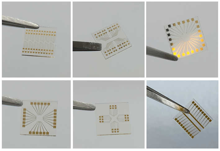
Photolithography with Platypus Technologies
Platypus Technologies offers several metal coating services for a range of applications. One of those services includes photolithography, frequently used for biosensor chips and gold films of various substrates. Photolithography offers many benefits, from repeatability to low cost, but it is difficult for some labs to achieve because it requires an ultra-clean environment. This is where Platypus Technologies can help, as we offer this service in a Class 100 cleanroom, which ensures high-quality surface patterning and outstanding repeatability.
If your application requires surface patterning, please contact us today for more information about Platypus Technologies’ photolithography processes and services.