Using Photolithography for Surface Patterning
What is Photolithography?
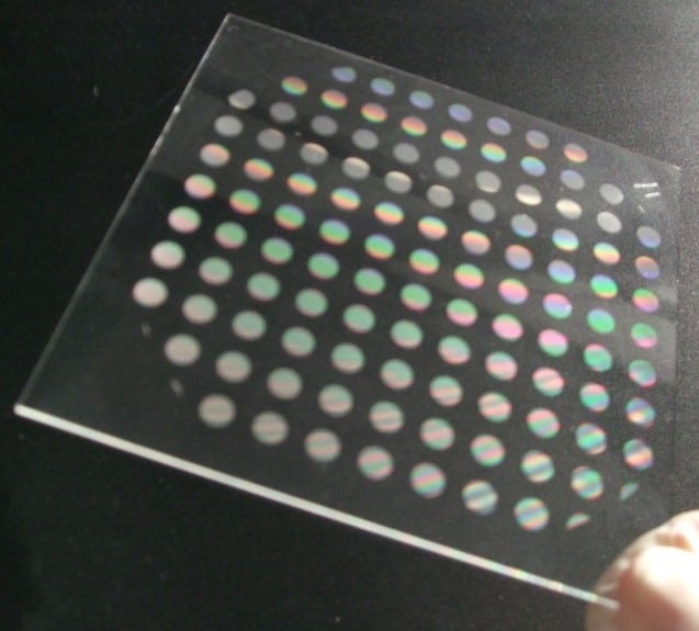
Photolithography, sometimes known as optical lithography or UV lithography is a process that is used in microfabrication for surface patterning parts of a thin film or the bulk of a substrate. Photolithography uses light to transfer a geometric pattern from a photomask to a light-sensitive chemical photoresist or simply resist on the substrate.
A series of chemical treatments are then used to engrave the exposed surface to create a pattern in the material. Alternatively, it may enable the deposition of new material in the desired pattern on the material beneath the photoresist.
Photolithography has some similarities to photography in the sense that the etching is formed by exposure to light either directly or indirectly using a projected image. Photolithography is comparable to the high precision version of the technique employed to create printed circuit boards.
The photoresist pattern is used in surface patterning by transferring it to a thin metal film using one of two techniques:
Wet Etching, in which the photoresist is deposited and patterned on top of the metal film. Those areas that are not covered by the film are then removed using chemicals.
Metal Lift-Off, a process in which thin metal film is placed on top of the patterned photoresist, then the photoresist itself is dissolved to reveal the pattern of the metal film.
The Benefits of Photolithography Surface Patterning
Photolithography is used in surface patterning for creating extremely small patterns and allows for exacting levels of control over the shape and size of the objects it creates. Photolithography can also create patterns over an entire surface in a cost-effective manner. However, photolithography always requires a flat substrate to start with and extremely clean operating conditions. This form of surface patterning is highly cost-effective and efficient.
Main Applications of Surface Patterning via Photolithography
Surface patterning via photolithography forms integrated circuits and other internal computer parts. It can be used for producing nanites and microscopic computer systems and any applications that require small surface patterning.
Is Photolithography the Right Surface Patterning Technique for Your Application?
There is a range of surface patterning techniques, including photolithography that can be used. Photolithography has many benefits, from its precision to how cost-effective it is.
Platypus technology offers a range of metal coating services that are suitable for both industrial and academic applications. Platypus has a Class 100 cleanroom and photolithography workflow allowing for excellent repeatability and high-quality surface patterning.
Platypus surface patterning has been used for new biosensor chips, surface platinum electrodes, gold films on flexible substrates, and more. If you would like to find out more about Platypus’ photolithography surface patterning services, get in touch with the team today.