An Overview of the Fabrication Processes for Interdigitated Electrodes
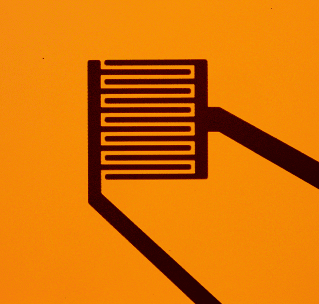
Interdigitated electrodes (IDEs) are fabricated through the process of combining two separately addressable electrode arrays, such that the resulting electrode structure is in a zipper-like or comb-shaped arrangement.
Used throughout a diverse range of electrochemical sensor applications, interdigital transducers (IDT) built from IDEs are favored for the relative ease and low cost of the fabrication process, as well as the high sensitivity of the specialized sensors built around IDE components.
Learn More About Platypus Technologies’ Interdigitated Electrode Products
The Advantage of Interdigitated Electrode Configurations
The comb-like shape of the interdigitated electrode configuration enables the electrodes to adhere to each other, or essentially infuse together. This infusion process minimizes the distance between the electrodes when compared to simpler, more conventional thin-film microlithography architectures.
The end result is a sensor that is more precise, capable and reliable. The reduced distance between electrodes enables quicker ion diffusion that yields a better data rate capability along with higher power density and performance.
The Fabrication Processes Behind Interdigital Transducers
There are three primary microfabrication processes used in the precision manufacturing of interdigitated electrode structures.
Laser Etching:
With laser-etched IDTs, a precise photomask is digitally designed and written onto the substrate through the laser-removal of material (typically chromium) deposited on the surface.
Reactive Ion Etching:
Reactive ion etching (RIE) is a method of dry etching that utilizes a chemically reactive plasma to carefully remove material that has been deposited on the underlying substrate. The plasma is electromagnetically generated via powerful RF frequencies which forces ions to essentially “attack” and remove surface material.
Inductively Coupled Plasma:
Inductively coupled plasma (ICP) is generated via powerful electromagnetic induction, yielding an extremely high-density, contamination-free plasma source. The IC plasma is then used to precisely etch the surface of the substrate and yield an interdigitated architecture.
Custom-Fabricated Patterned Electrodes for an Array of Applications
Platypus Technologies’ expertise in the fabrication of interdigitated electrode transducers extends to a diverse range of sensor applications, including:
- MEMS biosensors (bioMEMS)
- Chemical sensors
- Biosensors
- Lab-on-a-chip devices
- Field-effect transistors
If your application requires a more specialized sensor solution, contact us to discuss how Platypus Technologies can develop your custom-patterned microelectrodes. Our state-of-the-art production facility has the capability to coat and pattern various metals (Au, Ag, Pt, Ni, Ti, Al) on silicon, glass, or flexible substrates. See our Services page for additional information.