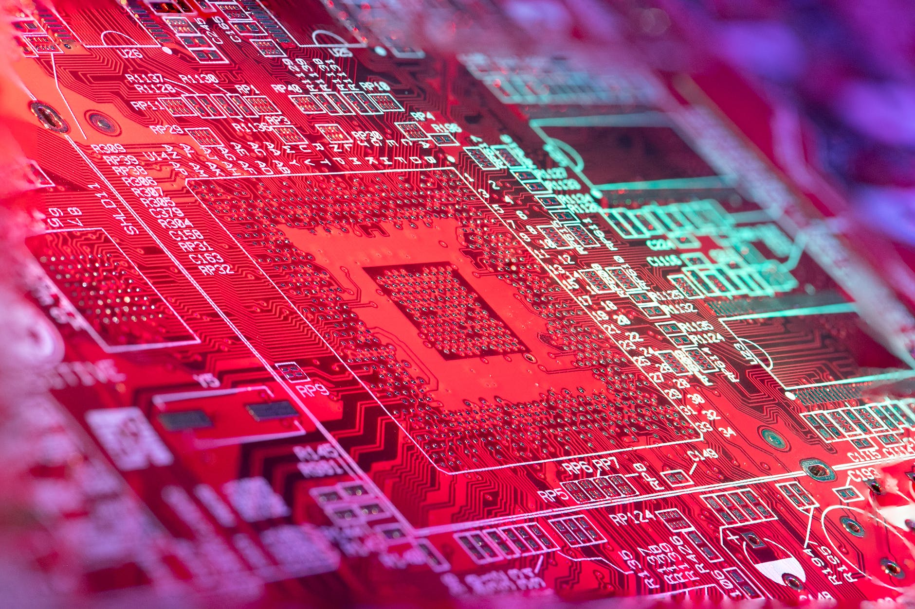
Photolithography: Applications in Microfabrication
Photolithography is an important microfabrication technique used to pattern substrates for modern electronics, sensors, and microfluidics. It is a precise form of custom surface fabrication where the interface of a wafer is coated with a light-sensitive polymer known as a photoresist. The coated wafer is then exposed to light which is selectively attenuated by a mask, leaving behind a latent image which is chemically, physically, or optically etched to provide a permanent micro-structured pattern on the wafer’s surface. Coupled with metal deposition and etching techniques, photolithography is a versatile method for fabricating microstructures for optics, chemical and bio-sensors, and microfluidic devices.
Understanding Photolithography
Moore’s law suggests that dense integrated circuits (ICs) double the number of on-chip transistors every two years. Given that photolithography currently enables manufacturers to develop ICs with feature resolutions as low as a single micrometre (µm), it naturally follows that printed electronics development must either slow down, or enhance to the point of nanoscale processing.
Nanotechnology is one of the next great frontiers of microfabrication, but engineers are still only scratching the surface with what is possible at the microscale. Photolithography has a critical role to play in pushing the lithographic letter, specifically techniques like including i-line exposure with ultraviolet (UV) wavelengths—typically 365nm. Additionally, photolithography service providers are increasingly able to offer greater expertise with challenging epoxy and metal lift-off resists—a prerequisite for microscale surface fabrication.
All this enables photolithography solutions that empower engineers and scientists with new levels of surface resolution and precision.
Applications of Photolithography
Patterned Gold Electrodes
Photolithography plays a key role in the generation of patterned gold electrodes which benefit from high topographical uniformity and lateral precision, plus the inherent conductivity of gold, to yield high-performance electrical elements for advanced analytical applications and sensor development. Key development areas for patterned gold electrodes include unique biosensors comprosed of advanced microelectromechanical systems (MEMS) – or bioMEMS.
Optical Filters
Interference filters are crucial elements in photolithographic workflows, particularly aftermarket i-line systems requiring a stable monochromatic light source to be reliably resolved. Yet photolithography also plays an increasingly important role in generating OEM filters with selective, high resolution surface patterns. Additionally, pristine gold substrates are often prepared for use in optical microscopy and advanced imaging techniques like surface plasmon resonance (SPR).
Microwells and Micropillar Arrays
Biological and cellular imaging increasingly make use of microwell arrays consisting of patterned substrates that enable a range of functionalities for life science applications. Photolithographically generated honeycomb arrays are useful for stabilising liquid films for particle separations, for instance.
Photolithography Services from Platypus Technologies
At Platypus Tech, we understand the cost and time burden associated with highly parallel workflows like substrate patterning. Yet the need for high-precision custom surfaces often puts the onus on end-users to find a solution that pushes beyond the capabilities of readily-available solutions. That is why we have developed a truly customizable photolithography service to satisfy the needs of users in various areas of research and development (R&D). Interested in learning more? Ask about our partnership opportunities today.