Advantages and Disadvantages of Photolithography
Photolithography, also known as optical lithography, is a microfabrication technique that uses light to produce precisely patterned thin films over substrates such as silicon wafers. These patterned films typically protect selected areas of the underlying substrate during subsequent processing, such as etching or metal deposition.
What is Photolithography?
Photolithography involves several steps. First, the substrate is coated with a photoresist: a thin, flat layer of a light-sensitive substance. Next, the photoresist is exposed to a precise pattern of intense (typically ultraviolet) light. This is typically achieved using a “photomask” which blocks some parts of the light, while letting through others, although in some applications, the pattern is projected directly onto the photoresist. Exposure causes parts of the photoresist to undergo a chemical change.
The final step of the photolithography process is developing. The photoresist is exposed to a special “developer” solution that preferentially dissolves parts of the photoresist depending on their exposure to the intense light. A “positive” photoresist becomes soluble when exposed, causing the exposed parts to dissolve during the developing process. With a “negative” photoresist, unexposed parts remain soluble while exposed parts become insoluble.
Photolithography is typically followed up by additional processing. For example, wet chemical etching may be used to remove layers of substrate which are not protected by the patterned photoresist. In metal lift-off, the photoresist may be coated with a thin metal layer prior to developing to produce a patterned metal film.
Applications of Photolithography
The primary application of photolithography is the production of semiconductor devices by patterning silicon wafers. In these applications, photolithography is followed up by etching processes – typically plasma etching – where the patterned photoresist enables selective removal of parts of the substrate.
Other applications of photolithography include patterned gold electrodes for use in biosensing, highly selective interference filters for optics, and microwell arrays for bioscience applications. Read more about the applications of photolithography in microfabrication here.
Advantages of Photolithography
Photolithography can create patterns with extremely small features – down to a few tens of nanometers – while also enabling incredibly precise control over feature geometry. Photolithography is also comparatively fast, capable of creating patterns over an entire silicon wafer with relatively low cost.
Photolithography is also versatile: it’s commonly used to pattern various materials, including glass, silicon, and even flexible substrates.
Disadvantages of Photolithography
Though photolithography is extremely useful in research and engineering applications, it does have some limitations. From a technical standpoint, there are only a few challenges: photolithography is only suitable for perfectly flat substrates, and it is fundamentally limited by the wavelength of light used (though there are ongoing efforts to overcome the “diffraction limit” of photolithography for next-generation semiconductor applications).
The primary drawbacks of photolithography are practical rather than technological. Firstly, photolithography equipment is extremely expensive – a trait shared by virtually every piece of equipment used in semiconductor manufacturing. In addition, photolithography can only be carried out in an environment free from airborne particulate or chemical contaminants, meaning photolithography must be conducted in a cleanroom.
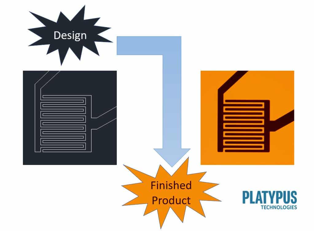
Photolithography Services from Platypus Technologies
Understandably, investing in cleanroom facilities and photolithography equipment is not a practical consideration for all laboratories or manufacturers. That’s why we offer a comprehensive range of photolithography services for the fabrication of several types of patterned surfaces.
The Platypus Technologies photolithography lab is equipped with a 365-nm highly collimated exposure system capable of 5-µm minimum feature resolution on circular substrates up to 6” diameter and square substrates up to 4” x 4”.