Key Steps in Fabricating Molds for Microfluidic Devices
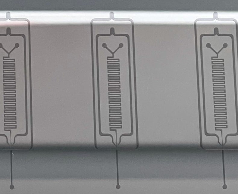
Microfluidic devices are becoming more popular because of their ability to precisely manipulate small quantities of fluids through narrow channels, which is beneficial in a range of applications and scientific fields, including biology, chemistry, and medicine. Most microfluidic devices rely on standard photolithography as a microfabrication technique to pattern substrates and process photoresists for the electronics industry. However, soft lithography is a complementary addition to photolithography that can process various materials, such as gels and polymers.
Soft lithography is not an independent method of microfluidic device fabrication. It must be paired with another lithography technique, which is often photolithography or e-beam lithography, to create the necessary mold or stamp. In this blog post, we look at the key steps involved in fabricating SU-8 molds for soft lithography, which is used to produce microfluidic devices.
SU-8 Mold Fabrication
This post will look at the process for producing SU-8 epoxy resin molds with a silicon wafer. However, it is important to mention that other methods and materials are available, depending on preferences or suitability.
Wafer Preparation
Before an SU-8 photoresist is added to a wafer, the water must be prepared. This stage involves cleaning the wafer with acetone and heating it to remove all surface moisture. After heating the wafer, the SU-8 resin should connect better with the substrate.
Spin Coating
In order to create the mold, you need to create a photoresist layer. The most common method of doing so is spin coating, which produces the required uniform layer on top of a substrate. A pool of SU-8 photoresist is placed in the middle of the substrate, which is on a rotating platform. The thickness of the photoresist layer can be determined by the acceleration and rotation speed of the platform.
Soft Baking the Photoresist
Once the photoresist layer has been through the spin-coating process, the soft baking process is used to evaporate the solvent and harden the SU-8 photoresist. This is the first out of three baking processes involved in developing a mold.
Photomask Alignment and UV Exposure
A photomask is aligned with the substrate to ensure the correct pattern can be created on the surface. SU-8 is a negative photoresist, which means that it will become hard when exposed to UV light, and the part not exposed will dissolve.
Post-Exposure Baking
The second baking process happens after the substrate is exposed to UV light. The photoactive components are activated during UV exposure, but energy is needed for the reaction to develop further. In post-exposure baking, that required energy is produced and helps develop the mechanical properties of the substrate.
Development
The wafer is immersed in a solvent to reveal the design patterned on the substrate, as well as dissolve the ares of the photoresist that were not exposed to UV light.
Hard Baking
Hard-baking is the third baking process in fabricating a SU-8 mold and is conducted to increase the mechanical properties of the substrate and reduce the chances of the material cracking. It’s worth mentioning that this stage is optional.
Checking
Finally, the finished SU-8 mold must be checked to ensure it is suitable for its intended application and meets any regulatory requirements. This is usually conducted under a microscope but can undergo additional observation under an optical or a mechanical profiler.
Platypus Technologies
Platypus Technologies offers a range of photolithography services and provides negative and positive photoresists (including SU-8 wafers) for various applications across the electronics industry.
Contact a member of Platypus Technologies today to learn more about SU-8 photolithography or fabricating SU-8 epoxy molds.