Patterning ITO Thin Films: Fabricating Conductive Transparent Devices
In this blog, we will delve into the world of ITO thin films and discuss how photolithography and wet etching techniques can be utilized to create transparent conductive electrodes, radio frequency (RF) devices, and more.
What is Indium Tin Oxide (ITO)?
Indium Tin Oxide (ITO) is a unique material made from a mixture of indium oxide and tin oxide. This compound is widely used in various industries due to its impressive properties, which include optical transparency and electrical conductivity. ITO is commonly found in applications such as touchscreens, solar cells, and OLED displays.
There are several advantages to using ITO thin films in various applications:
- Optical properties: ITO thin films exhibit high transparency in the visible light spectrum and low reflectivity, making them ideal for display and touch panel applications.
- Electrical properties: These films offer low electrical resistance and high carrier mobility, which contribute to their excellent performance as transparent conductive materials.
- Durability and stability: ITO thin films possess excellent stability under various environmental conditions, making them suitable for long-term use.
Patterning ITO Thin Films via Photolithography and Wet Etching
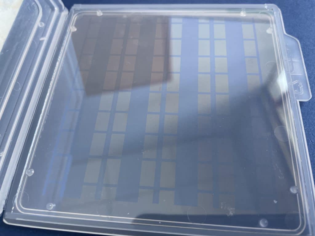
To create patterns on ITO thin films, Platypus Technologies utilizes photolithography and wet etching techniques.
Photolithography is a process that uses ultraviolet (UV) light to create patterns on a light-sensitive coating called photoresist, which is deposited on a substrate. A mask is placed on top of the photoresist to block UV light from certain areas, leaving only unmasked regions exposed to light. The pattern is then revealed by removing unprocessed areas using a suitable solvent. The photoresist then protects some areas of the ITO film, while exposing other areas.
Wet etching involves the removal of unprotected ITO areas using specific liquid chemicals.
Learn more about patterning thin films
Application of Patterned ITO Thin Films
Patterned ITO thin films find uses in a variety of applications:
- Transparent conductive electrodes: These are used in touchscreens, OLED displays, and solar cells, where both transparency and conductivity are required.
- Electrode arrays: ITO thin film electrode arrays are utilized in biosensor applications for detecting chemical and biological substances.
- Interdigital transducers: These devices are used in surface acoustic wave (SAW) filters, which are commonly found in RF communication systems.
- Radio frequency (RF) devices: Patterned ITO thin films can be employed in the fabrication of antennas, filters, and other RF components.
Conclusion
ITO thin films, with their unique properties, are paving the way for innovative applications across various industries. By using photolithography and wet etching techniques, these films can be patterned to create transparent conductive electrodes, RF devices, and more. Platypus Technologies is your go-to partner for reliable and high-quality solutions in the field of ITO patterning. If you have any questions or need assistance, feel free to contact us, and our team of experts will be more than happy to help.