What are Patterned Electrodes?
Additive manufacturing (AM) is a growing engineering paradigm that enables technicians to produce a wide range of intricate, prototypical parts. Among these are small-scale patterned electrodes for scientific micro-electromechanical systems (MEMS).
Printed Electrodes—The Basics
Generally, integrated circuitry for sensing elements is generated via selective sublimation using a photoresist that is exposed to electron or X-ray beams. There are many steps to the conventional printing process including pre-treatment with photo-resistant solvents and ex-situ modification (i.e. chemical etching). This can be problematic for patterned electrodes intended for biosensing or chemical sensor chips where negligible contamination is needed to ensure quality of results. Additionally, the surface morphology of patterned electrodes can have a demonstrable impact on electrical performance, thus affecting detection efficiency.
Nanopatterned electrodes produced via deposition are subsequently an attractive prospect for electrochemical assays, bioMEMS, and other extremely high-sensitivity electrical platforms. They can now be generated using a raft of AM techniques, from screen printing to e-beam evaporation.
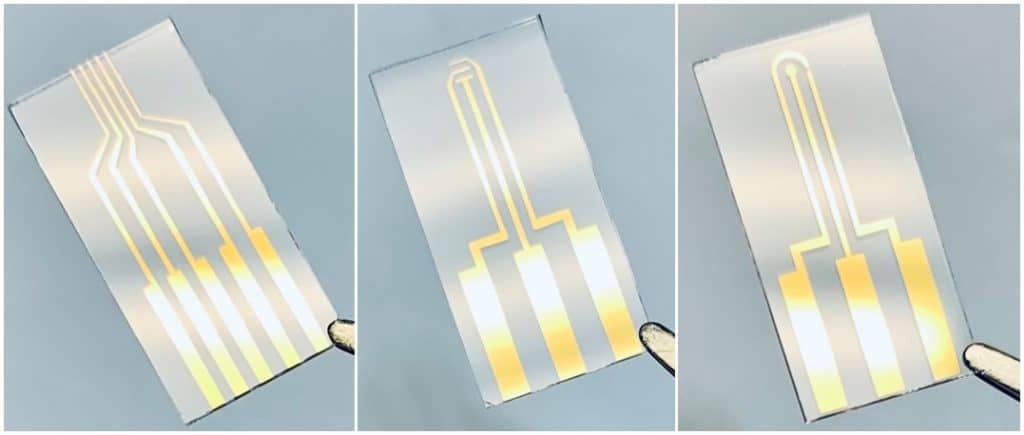
E-Beam Evaporation for Patterned Electrodes
Electron beam physical vapour deposition (EBPVD) is one of the preferred methods of producing highly conductive three-dimensional patterns on functional substrates with low surface roughness and high lateral fidelity. Using ultra-clean glass substrates with a titanium adhesion layer and a completely pure (<99.999%) gold anode—plus tightly controlled deposition rates—EBPVD can yield high-sensitivity patterned electrodes with low roughness down to the nanoscale. The optical transparency of the glass substrate enables easy visual sensing of the conductive gold layer, which is strongly and cleanly adhered to the substrate by the chemically-pure titanium intermediary. This offers numerous benefits for in situ visualisation of experimentation via microscopy or spectroscopy.
At Platypus Technologies, we have fine-tuned our e-beam processing capabilities to ensure excellent repeatability which has enabled us to launch a proprietary line of research grade gold patterned electrodes. These include:
- Resistivity electrode: A 5-probe microelectrode ideal for measuring sheet resistance, impedance, or conductivity of various materials.
- Three probe electrode: Designed for bio- and chemical sensor R&D.
- Disk electrode: Intended for electrochemical impedance spectroscopy (EIS) or cyclic voltammetry.
Patterned Electrodes from Platypus Technologies
Although we offer many off-the-shelf solutions for scientific imaging, the Platypus Tech specialty is custom coating for proprietary applications. Contact us today if you would like more information about our ready-to-order patterned electrodes, or if you are looking for a bespoke solution to any bioMEMS or chemical sensing problem.