Scanning Tunneling Microscopy of Ultra-flat Gold Surfaces
New STM imaging study reveals stunning atomic-scale details on Ultra-flat Gold Surfaces.
Ultra-flat gold surfaces enable high signal-to-noise imaging for AFM and STM applications. Because of their ultra-smooth topography, these surfaces have been used to study 2D materials, single strands of DNA, self-assembled monolayers, nano-plasmonic devices, and cell membrane monolayers.
In a new imaging study, Dr. Árpád Pásztor from the University of Geneva, in Switzerland, performed scanning tunneling microscopy (STM) measurements of Ultra-flat Gold Surfaces by Platypus Technologies. The samples consisted of freshly-stripped gold surfaces grown on silicon wafers (AU.1000.SWTSG). These experiments were carried at low temperature (77 K) under ultra-high vacuum conditions. The resulting high-resolution images, which were kindly provided by Dr. Pásztor and are reproduced below with permission, reveal stunning new details on the ultra-flat gold surfaces by Platypus Technologies.
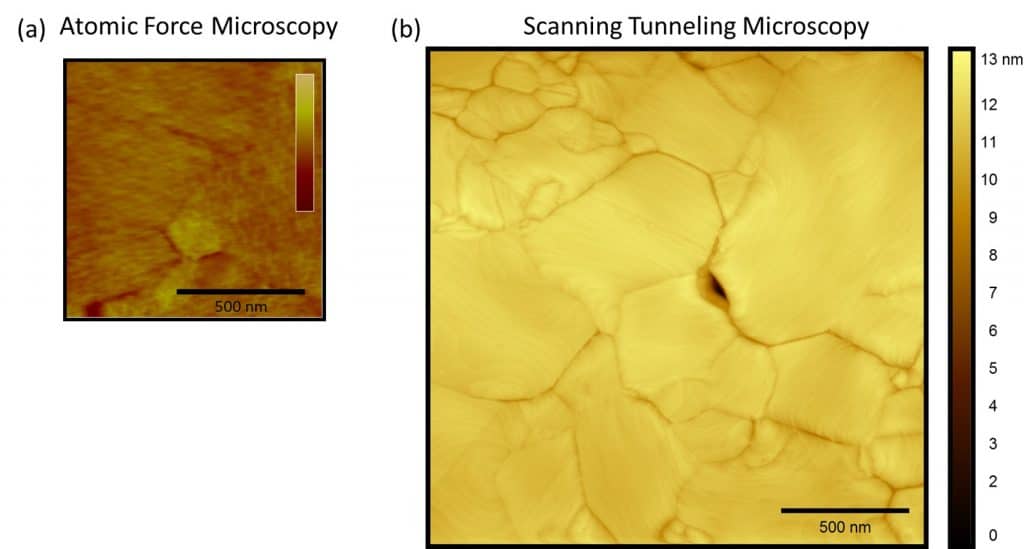
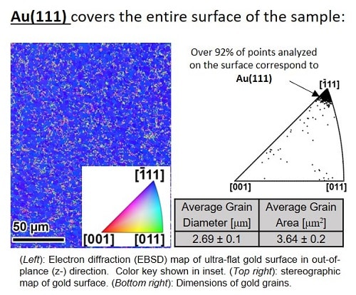
Initial inspection of the STM images reveals gold grains with dimensions of several hundred nanometers. A prior study with electron backscattering diffraction (EBSD) analyzed areas of 160 μm x 200 μm of the ultra-flat gold surface, measuring the average diameter and area of gold grains as 2.96 μm and 3.64 μm2, respectively. Inspection of the height scale (right of STM image, Figure 1b) confirms that the surface exhibits uniform height topography over the entire area analyzed. Except for grain boundaries, the entire surface has similar height and height variations are within one (1) nanometer.
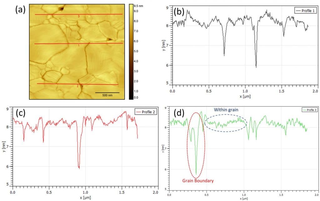
Linear scans of the ultra-flat gold surface provide quantitative measurements of the surface height. Figure 2 presents a representative STM image and three height profiles from linear scans. This data reveals that within each grain of gold, the surface height variation is significantly less than 1 nanometer, and the decrease in height that corresponds to grain boundaries is only ~1 – 2 nanometers. For comparison, the thickness of the cell membrane is ~4 nanometers.
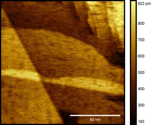
Next, the imaging study characterized nanometer-scale height variations of the gold surface within each grain (Figure 3). The images reveal that each grain is composed of several stacked terraces of gold. By close inspection of the images, we observe that the terrace-to-terrace height difference is ~0.2 nanometer, a value that is consistent with the within-grain height variation measured by the linear scans in Figure 2.
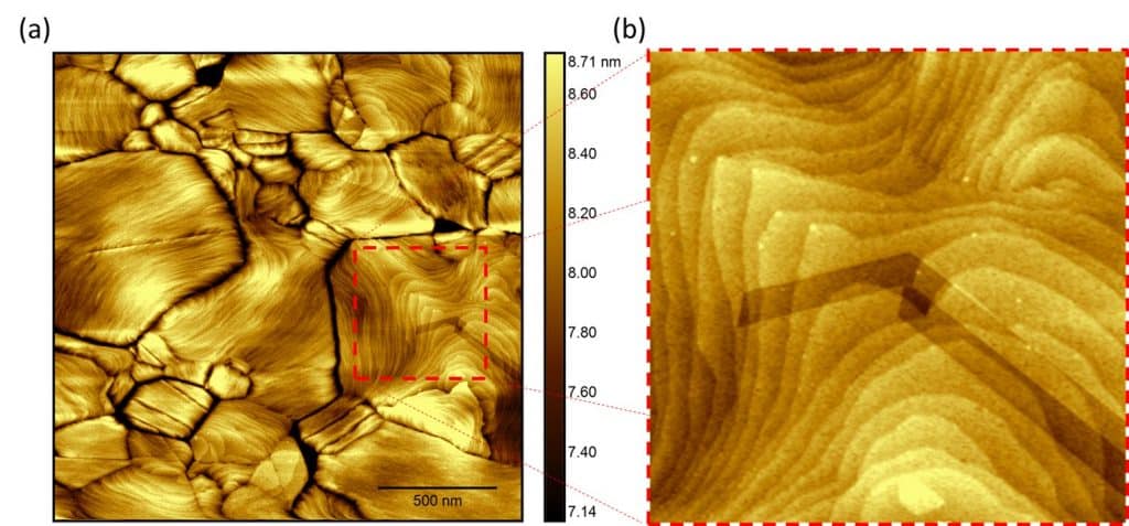
A high-resolution STM image of a 100 nm x 100 nm area within a gold grain is presented in Figure 4. From this image, single terraces of gold can be clearly observed. The terrace at the center of the image measures approximately 3,000 nm2. Additionally, we observe that the terrace-to-terrace variation in height is in the order of a few hundred picometers. For comparison, the diameter of gold atoms in metallic bonding is 288 picometers. Thus, we hypothesize that the observed sheets within each grain (Figures 3 and 4) correspond to atom-thick terraces of gold, and that each terrace corresponds to a uniform plane of gold atoms.
In conclusion, high resolution STM images of ultra-flat gold surfaces reveal exquisite detail of the surface. The images reveal large grains of gold with uniform surface roughness over the entire area analyzed. Each grain is composed of gold terraces with single-atom thickness.
Learn more about Ultra-flat Gold Surfaces
Credits: All STM images and data were generously provided by Dr. Árpád Pásztor from the University of Geneva. The marketing team at Platypus Technologies composed and formatted the contents of this blog. Questions or Comments? Please contact us