How Thin Films Factor into Surface Science
Thin films are used in a wide range of advanced applications in surface science, and studies surrounding thin films have significantly advanced solid state chemistry and physics. Surface science relates to any surfaces, interfaces and their applications and any research or development in the field. Thin films play a large part in surface science, and this blog post aims to cover how and why.
How Are Thin Films Used In Surface Science?
There are a variety of applications in which thin films make positive contributions. These include optoelectronic, photonic and magnetic devices, wireless communications, video systems and flat panel coatings. Additionally, other typical applications are:
● Advanced optical applications
● Biomedical devices
● Fiberoptic systems
● Industrial laser systems
● Medical electronics
● Semiconductor manufacturing
The properties of thin films can be controlled by how thick the film is. Adjusting the thickness of a thin film can impact the costs, production yields and results of the film’s application. Tight control of thin film deposition is critical to achieving the required film thickness.
What is Thin Film Deposition?
Thin film deposition is where thin film coatings are deposited onto a substrate material, which is a crucial part of the manufacturing process of many devices. Thin film deposition takes place to create a coating for another substrate. These coatings can be made from many film materials which in turn provide different characteristics. These characteristics can then be used to change or improve the performance of the thin film.
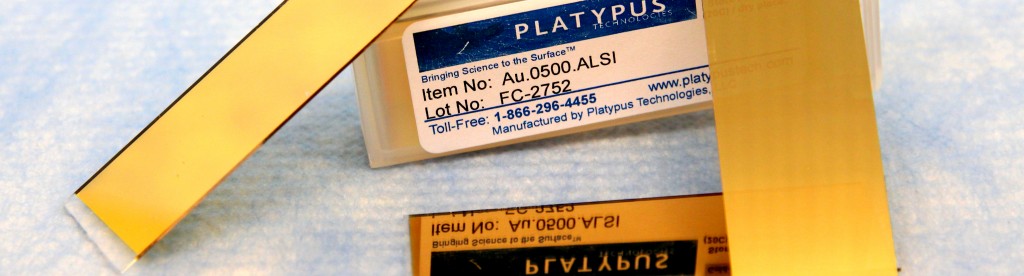
Pristine Gold Thin Films
Customers worldwide prefer Platypus gold thin films on glass, silicon and mica because they are fabricated by e-beam evaporation with titanium adhesion layers. Films are guaranteed chrome-free.
The deposition process can be carried out in multiple ways depending on the performance and production requirements your application needs to succeed. For example, if a thin film can withstand high temperatures and be corrosion resistant, physical vapor deposition (PVD) would be an ideal technique. However, thermal evaporation would be more appropriate if the film is used in OLEDs or solar cells.
Additional thin film deposition methods include E-beam evaporation, ion beam sputtering, magnetron sputtering and pulsed laser deposition (PLD).
Benefits of Thin Films
Thin films have advanced rapidly in recent years owing to the efficiency and various properties that support a range of applications. As the name suggests, some of the benefits of thin films are that they are thin and suitable for mechanical data storage. Other benefits include:
● Highly efficient: In solar energy, electronics and construction, thin films can be made to suit a range of requirements.
● Improves surface of a material: These include absorption, corrosion, electrical properties, hardness, thermal conductivity and more.
● Low-cost: As they can be constructed with low-cost materials, this makes them more cost-efficient to use in applications.
● High yield strength: Yield strength can be modified by changing the properties of thin films. However, maintaining the film thickness is key to stabilizing the yield strength.
Platypus Tech
Platypus Tech specializes in creating custom metal coatings via e-beam evaporation. Through this vapor deposition process, we retain a high level of control over film thickness, resulting in high-purity thin film coatings that are both highly reproducible and uniform. If you would like more information on our thin film coatings, please do not hesitate to contact us today.