How are Silicon Wafers Used in Electrochemistry
Silicon wafers are materials that are used for the production of semiconductors. They can be found in many types of electronic devices that are used in everyday life. Silicon wafers are super-flat disks that are refined into a mirror-like surface, they are extremely clean and free from impurities and micro-particles.
Silicon wafers are particularly well suited to use in electronic devices because electrical currents can pass through silicon conductors than many other materials. Here we will explore more about the uses of silicon wafers in electrochemistry and some of their key characteristics.
Silicon Wafers for Semiconductors
Silicon wafers are well suited for use in semiconductors because of their high mobility at room temperature and high temperatures. Silicon wafers are ultra-clean and free from microparticles, this makes them the perfect material for the substrate of the modern semiconductor.
Silicon Wafers in Other Electronic Devices
Semiconductors such as silicon wafers can also be used to produce chips and microchips for use in electronic gadgets. Silicon wafers are unique in their approach to electrical currents, making them well-suited to use in integrated circuits. Integrated circuits act as commands for specific actions in a range of electronic devices.
Silicon wafers are the main element in integrated circuits as they are a composite of a range of electronic elements brought together for a specific function.
Silicon Wafers and Electrochemical Impedance Spectroscopy
EIS is an intricate and sophisticated form of electrochemical research, offering extensive insight into phenomena such as surface sensitivity and electron transfer resistance. EIS is achieved by immobilizing an analyte on a semiconducting surface whilst under applied voltage. The response is then measured.
Sometimes silicon wafers need to be modified with a secondary material to be used in EIS. One solution for this is using ultra-thin gold coatings which offer outstanding planarity.
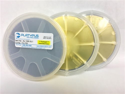
Gold-Coated Silicon Wafers
Precision imaging is increasingly reliant on gold surfaces for a range of biochemical phenomena. Gold surfaces are ideal for atomic-scale observations partly due to their near-total reflectivity in the IR region and their adsorption properties.
Platypus Technologies have a range of custom gold-coated silicon wafers for use in electrochemistry. All substrates are based on electron beam physical vapor deposition of high-purity gold targets If you would like to find out more about how gold-coated silicon wafers can be used in electrochemistry applications, contact us today!