An Overview of the Photolithography Process
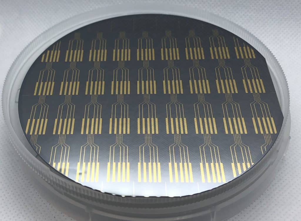
Photolithography is a fabrication process used in the production of patterned thin films for precision applications such as microelectronics, biosensors, and custom patterned electrodes. The process utilizes ultraviolet (UV) light to expose a minutely detailed pattern within a light-sensitive photoresist coating.
The coating is deposited on a substrate material and a mask is placed atop the photoresist. UV light therefore interacts only with the areas of the photoresist that are left exposed underneath the mask. Once the mask is removed, a precise geometric pattern remains on the substrate surface, formed via exposure to the UV light.
Platypus Technologies stocks both negative and positive photoresists for diverse applications. Based in Madison, Wisconsin, we are one of the Upper Midwest’s leading providers of innovative photolithography services.
A Breakdown of the Typical Fabrication Steps in Photolithography
The photolithography process can be broken down into three overarching procedures: coating, exposure, and development.
The coating process involves preparing the substrate with an appropriate photoresist layer. The substrate is then exposed to UV light in order to create the custom pattern. Finally, the exposed photoresist material is dissolved or removed, leaving behind the unexposed pattern.
Surface Preparation
The substrate surface is carefully prepared before the photoresist material is applied. Virtually all traces of contaminants must be removed to ensure proper adhesion. Additionally, adhesion promoters can be added to further ensure coating quality and consistency.
Photoresist Coating
After it has been properly cleaned and prepared, the substrate is coated with the required photoresist material.
The Pre-Bake Process
The substrate is then pre-baked or soft-baked in order to evaporate any excess photoresist coating solvent.
Photo Masking and Alignment
Using state-of-the-art digital imaging systems and other specialized photolithography equipment, the substrate and photomask are precision-aligned with the UV light source to ensure proper exposure.
Exposure and Development
In the exposure phase, the substrate is subjected to UV light, exposing the pattern underneath the photomask. While the process can be seen as analogous to exposing a conventional photograph with a film camera, the exposure process in photolithography uses far more advanced materials and exposure technology engineered to work precisely at a molecular level.
Post-Baking
After the pattern is exposed and developed it undergoes a post-baking or hard-baking process. This process hardens the developed photoresist material.
Processing, Stripping, and Post-Processing
Finally, the exposed photoresist material is dissolved or removed, leaving behind only the patterned material.
Learn more about Photolithography Services at Platypus Technologies.