Ultra-Flat Gold
Ready-to-use, Pristine Au(111) for Nanotechnology
Discover the pristine, ultra-flat gold(111) surfaces from Platypus Technologies, perfect for advanced nanotechnology applications. Our Template-Stripped Gold Chips offer unparalleled flatness, ideal for applications atomic force microscopy (AFM), Scanning Tunneling Microscopy (STM), Infrared Nanospectroscopy (nano-IR) and more.
Why Choose Ultra-flat Gold?
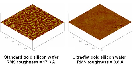
- Ultra-Flat Surface: Gold surface roughness approaches atomic flatness and enables high-resolution imaging and measurements at the nanoscale.
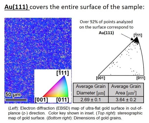
- Highly Oriented Gold: Uniform Au(111) domains through the entire area of the sample.
- Pure & Uncontaminated Gold: Our gold is shielded from the atmosphere until stripped from the template, ensuring a surface free from organics and atmospheric contaminants.
- Ready-to-Use: Say goodbye to the need for hazardous cleaning solutions or expensive equipment. Our chips are prepared for immediate use.
- Convenience at Its Best: With multiple chips per template, prepare fresh, clean, and ultra-flat chips in seconds before your next experiment.
Product Details – Template-Stripped Gold Chips
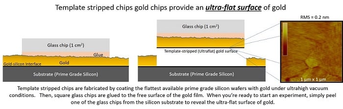
Designed for researchers, these chips are fabricated by coating the finest prime grade silicon wafers as templates. Then, 1-cm x 1-cm square glass chips are epoxy-glued to the surface of the gold. The gold surface you use is the one in contact with the silicon, so it is ultra-flat, highly-oriented Au(111), and protected from the atmosphere until you are ready to use it.
Immediately upon stripping, Template Stripped Gold Chips provide an RMS roughness approaching atomic flatness, with a water static contact angle substantially similar to that of a freshly-deposited, high-energy gold surface.
| Product | |
|---|---|
| Template-Stripped Gold Chips | BUY NOW |
Protocol – Follow our recommended procedure for peeling off glass chips.
Video Tutorial – Watch how to peel off chips from the substrate.
Analysis of Ultra-flat gold(111)
Scanning tunneling microscopy: High-resolution STM images of ultra-flat gold surfaces demonstrate large grains of gold with uniform surface roughness over the entire area analyzed.
Electron backscatter diffraction: Crystallography studies demonstrate ultra-flat gold films have a uniform Au(111) orientation that covers the entire area of the sample.
Applications
Ultra-flat gold surfaces are revolutionizing research areas:
- High-resolution characterization of single molecules and self-assembled monolayers (SAM) via AFM, STM and nano-IR.
- Pioneering work in self-assembly, single-molecule imaging, nano-contact printing, DNA origami, and nano-photonics.
Research Studies Utilizing Ultra-flat Gold Surfaces
- Phonon-Polaritons in flakes of h-BN
- Surface modes of periodic nanopatch metasurface
- Electron tunneling across plasmonic junctions
- Patterning of self-assembled monolayer (SAM)
- Enhancement in plasmonic nanoantennas
- Tip-enhanced Raman spectroscopy
Related: View additional published studies via Google Scholar