Wet Etching
Wet etching is a technique to pattern metal films into functional devices. A metal film covered with a patterned photoresist is submerged into a liquid that selectively removes exposed areas of the metal. This form of etching is an isotropic method, meaning that the metal is removed with equal rate all directions.
Immersion and spray etching represent the two main forms of patterning surfaces. Immersion wet etching involves wafers or glass panes that are immersed into an etchant solution for a specified time. Mild agitation is often applied to thoroughly cover the substrate surface. Followed by agitation is a rinsing and drying step. Spray etching occurs when an etchant is directly sprayed onto a substrate then rinsed with DI water. In general, wet etching is used to pattern features with sizes greater than 5 µm. The temperature and concentration of the etchant is used to control the etching rate of the metal.
Wet etching is commonly used for manufacturing microelectronic devices. This process is relatively fast due to high and controllable etch rates. It is also effective in removing material from larger areas. The disadvantage of wet etching primarily relies on the need for a liquid chemicals. Large amounts of etchant are often required in order to completely immerse a substrate, causing increased production costs. Most etchants also contain an acid which requires additional safety measures to be in place. However, compared to other techniques such as mechanical and dry etching, wet etching has favorable properties. Mechanical etching does not create a smooth surface due to excessive surface impacts. Dry etching often has low etching rates.
The variables involved in wet etching include a photoresist, metal, and substrate material (commonly glass or silicon). The etching rate can vary based on the type of chemical etchant used. Some etchants have a constant etch rate while others have a parabolic deviation. A process known as annealing can also influence the etch rate of glass. Annealing occurs when wafers or glass are heated to a defined temperature. It is used to remove impurities present on the surface and reduce internal stress. Common defects that can occur as a result of wet etching include notching on edges and pinholes. Pinholes can form from tensile stress and defects generated during metal deposition. Notches are created from stress induced cracking.
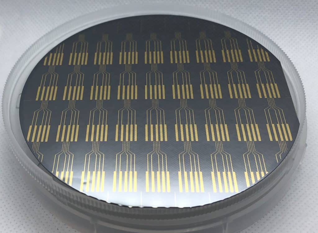
At Platypus Technologies two main forms of wet etching are conducted via immersion, gold and titanium etching. The gold etchant consists of potassium iodide in which the etching time is determined by the thickness of the gold. The gold etchant that is used has an etch rate of 2.8 nm/s at room temperature and doubles with every 10 °C increase in temperature. The titanium etchant has a much higher etch rate of 5 nm/s at 85 °C due to the presence of an acid within the solution. Etch rates are carefully determined in order to produce clean structures, and protocols have been perfected to produce high quality results for your next project.
Looking for custom devices?
Platypus Technologies fabricates custom devices for applications in biosensors, chemical sensors, and MEMS devices using techniques in photolithography and wet etching. Contact a member of our team to learn more.