Next-generation Photolithography
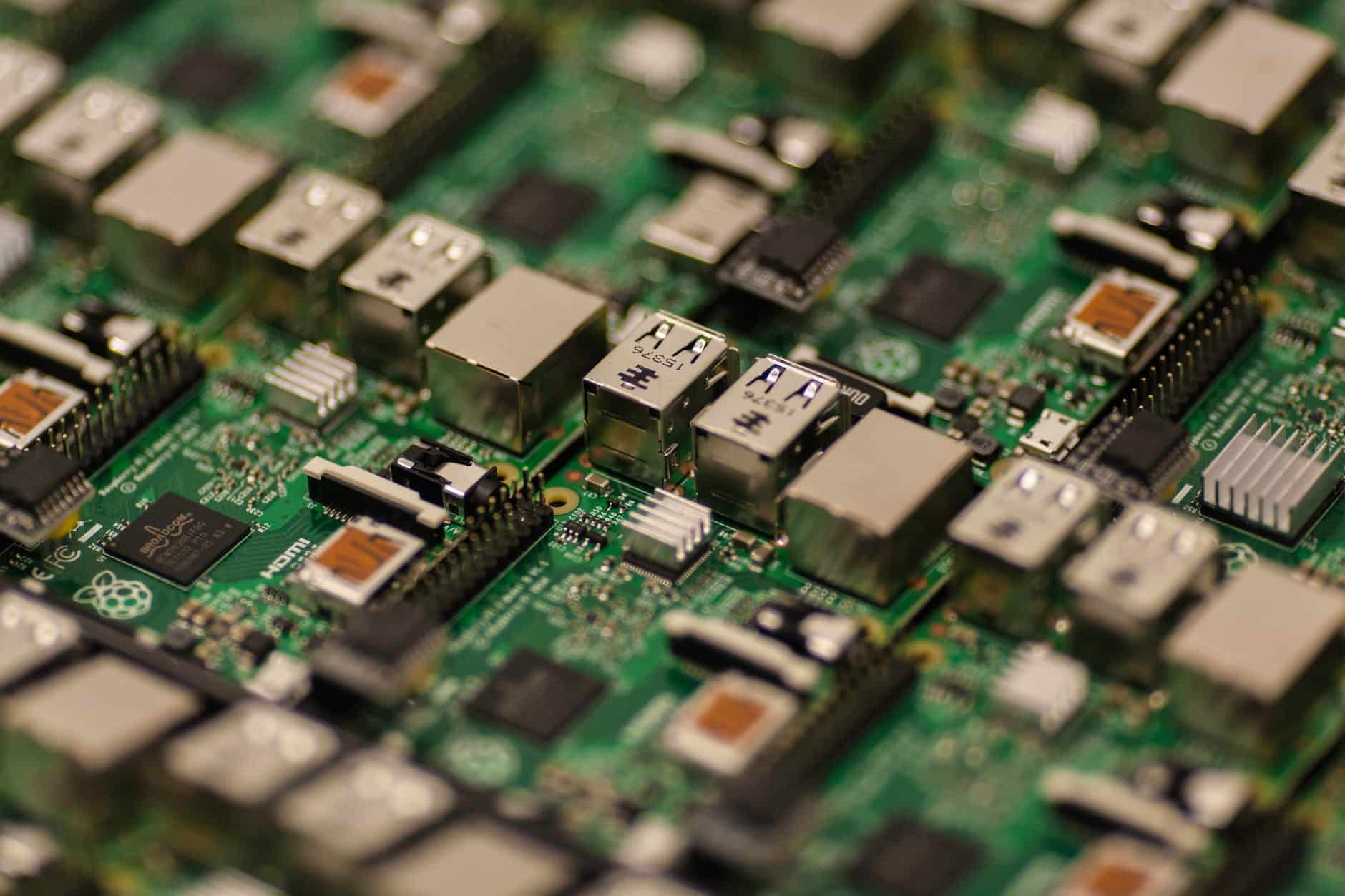
Photolithography techniques are used heavily in the integrated circuit industry. New industry standards have created a need for creating smaller features that enable lower power consumption.
Attainable feature sizes that can be achieved through lithography practices depend on the wavelength of light being used. Two common wavelengths include g-line (435 nm) and i-line (365 nm). Next-generation lithography (NGL) explores the possibility of attaining shorter wavelength in order to fabricate smaller features. However, shorter wavelengths also create decreased optical absorption and unwanted substrate reflections. Different NGL techniques are currently being explored and tested to enhance photolithography manufacturing processes. These include x-ray lithography, extreme ultraviolet lithography, and ion projection lithography.
X-Ray Proximity
X-ray lithography (XRL) is a shadow exposure method with specialized x-ray masks. X-ray masks are much thinner than traditional photomasks used in photolithography. Mask features must be made to be the same as those to be transferred onto a substrate material. The mask is exposed to x-rays where feature resolution depends on the diameter of the x-ray source, gap spacing between mask and substrate, and the distance from the x-ray source to mask. The mask conditions endured during exposure can cause mask deformation and vibrational bending. These distortions directly affect mask alignment and feature patterns. However, XRL smaller wavelengths (0.4-5 nm) are used to allow for an increase in electrical components, like transistors, to fit onto a substrate.
Extreme Ultraviolet Lithography
In extreme ultraviolet lithography (EUV) a plasma light source is used to penetrate through a reflective mask. EUV masks reflect light as opposed to transmitting it. The plasma source is used to create 13.5 nm photons which are gathered in an optical collector. This technique uses very small reflective optical systems with wavelengths that are shorter than desired feature dimensions. Multilayer mirrors, or Bragg reflectors, are used in EUV to create constructive interference. EUV allows for two-dimensional design features to be created and enables multiple patterning.
Ion Projection Lithography
Ion projection lithography (IPL) uses accelerated hydrogen ions to counteract diffraction problems. The heavy mass of ions produces less scattering leading to higher pattern resolutions. Highly UV resistant resists, such as PMMA, are used to reduce radiation damage and absorb the ions released during exposure. The mask material normally consists of a silicon stencil that has a carbon coating to prevent substrate swelling and distortions. In addition, masks are often patterned with holes to create a stencil mask. Electrostatic lenses are used to focus and deflect accelerated ions. Although IPL creates high resolution patterns, this technique is more expensive compared to conventional lithography techniques. In addition, longer processing times are common and substrate swelling can occur when using negative resists.
With a rising need for increasing the number of electrical components per substrate, it is important to rely on innovative engineering design services and modern photolithography techniques. The engineers at Platypus Technologies offer expertise to assist with mask design and custom photolithography manufacturing. Contact us today to help with your next project!