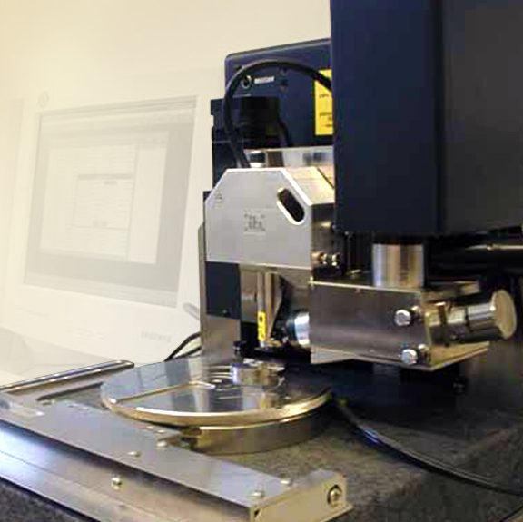
Fundamentals of AFM & Why Metal Surfaces Matter
What can we use to probe sample surfaces beyond visible light? Electron beams are ideal for powerful magnifications many orders of magnitude greater than that of optical microscopy. But when we are dealing with resolutions of nanometre (nm) and sub-nm proportions, resolving power isn’t the final word. This is partly because researchers are spoilt for choice when it comes to molecular-scale imaging solutions.
Say you want to assess both the morphological and topographical properties of a metal surface. Electron microscopy can provide detailed insights into phase structure, grain size, and so on. While the likes of scanning probe microscopy (SPM) can offer greater insights into the three-dimensional surface structures, even if your metal surface is topographically uniform at the nanoscale. Which technique do you choose?
Today, electron beams and physical scanning probes are often used in tandem for comprehensive sample analysis, saving you the agony of choice.
AFM: The Basics
Atomic force microscopy (AFM) is potentially the most popular microscopic method based on scanning probe technology. It complements the likes of scanning or transmission electron microscopy (SEM/TEM) by resolving even the subtlest topographical variations of highly smooth surfaces. Additionally, AFM can resolve a range of compositional qualities like adhesiveness, elasticity, magnetism, stiffness, and so on. This requires the use of specialized probe tips and precision-engineered substrates that promote high signal-to-noise ratios.
Here is a quick example: AFM has been identified as a useful method for evaluating the quality of self-assembled monolayer (SAM) printing on functionalised metallic surfaces. These unique organic molecules spontaneously assemble on surfaces via adsorption based on intermolecular and molecular substrate—molecule interactions. AFM can subsequently assess printing parameters and detect pattern errors of within a single molecule. However, this exceptional level of precision necessitates ultra-flat substrates – typically metallic surfaces like gold.
Template-Stripped Metallic Surfaces
In the context of AFM, flat means topographically uniform at the atomic scale. This isn’t an easy quality to achieve via conventional manufacturing methods like epitaxy or flame annealing. Although they can provide a decent level of flatness, this is limited to flakes with surface areas of no greater than two micrometers (µm2) which represents a prohibitively small substrate. Most applications require larger metallic surfaces than this.
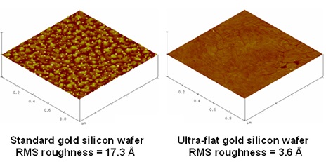
Template-stripping is a novel technique used to replicate the natural flatness of mica glass or polished silica in a metallic surface like gold. You deposit an adhesive intermediate on a glass/silicon chip and coat the template with a uniform gold thin film. The large area Angstrom-scale uniformity of the underlying substrates translates through to the metallic surface, yielding a highly-functional gold substrate with pristine design topographies.
This enables researchers to achieve the ultra-high resolution necessary for characterizing materials at the atomic range with negligible interference from substrate inhomogeneities or undesirable surface—tip interactions. Beyond the evaluation of SAMs, template-stripped metallic surfaces have proven ideal in single-molecule imaging, DNA origami, 2D materials characterization, and more.
Interest in using template-stripped gold for your AFM workflow? Contact a member of the Platypus Technologies team today for full design specifications and properties.