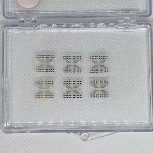
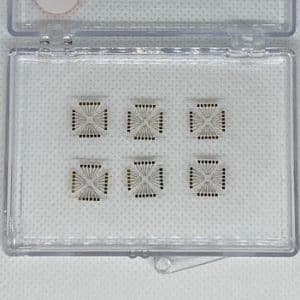
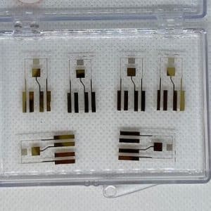
Description
Patterned electrodes from Platypus Technologies consist of gold thin-films deposited on glass via e-beam evaporation and micromachined via photolithography and wet etching. A titanium adhesion layer is applied between the gold film and glass substrate to improve mechanical stability.
Patterned electrodes are ideal for discovery-oriented research with applications in chemical sensors, biosensors, lab-on-a-chip, microfluidics, field-effect transistors, 2D materials, and more.
Features & Benefits:
- Low surface roughness: provides excellent sample-to-sample reproducibility.
- High-purity gold (99.999%): no need for dangerous/noxious surface cleaning steps.
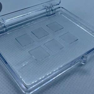
- Transparent glass substrate: easily visualize and manipulate your sample.
Custom electrode designs are available upon request. The team at Platypus Technologies has capabilities to coat and pattern various metals (Au, Ag, Pt, Cu, Ti, Al) on glass, silicon, ceramic or flexible substrates. See our services page for additional information.